
Android
Snapdragon 7+ Gen 3: सिर्फ processor नहीं, एक पूरा system-on-chip

फोन खरीदते वक्त “processor” शब्द सुनकर ज्यादातर लोग सिर्फ CPU के बारे में सोचते हैं। Snapdragon 7+ Gen 3 के मामले में यह सोच अधूरी तस्वीर देती है। यहाँ CPU अकेला काम नहीं कर रहा। Graphics के लिए अलग Adreno hardware है, AI workloads के लिए Hexagon architecture है, camera processing के लिए 18-bit Spectra Cognitive ISP है और 5G के लिए Snapdragon X63 Modem-RF System मौजूद है।
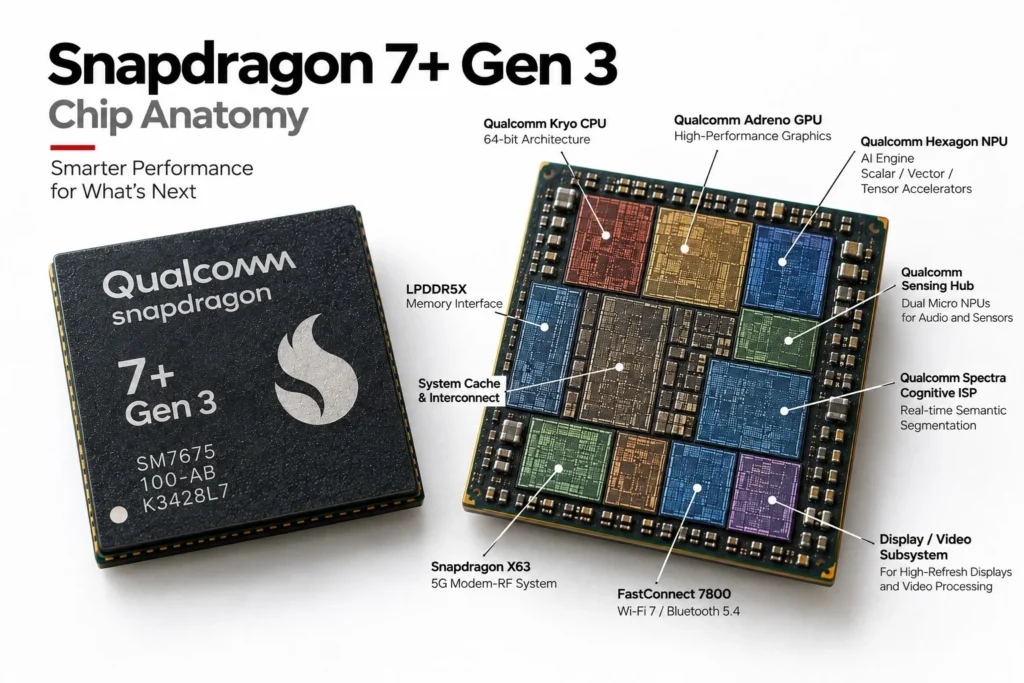
Qualcomm ने इस platform को 2024 में पेश किया था। यह 4nm process technology पर बनी है और इसका Qualcomm part number SM7675-AB है। Platform में 64-bit Kryo CPU, Adreno GPU, Qualcomm AI Engine, Sensing Hub, Spectra ISP, X63 5G Modem-RF, FastConnect 7800, LPDDR5X memory और UFS 4.0 जैसे अलग-अलग hardware blocks एक ही SoC architecture में जुड़े हुए हैं।
यही वजह है कि इसे केवल “processor” कहना थोड़ा misleading हो जाता है। Smartphone में processor शब्द अक्सर CPU के लिए इस्तेमाल होता है, जबकि Snapdragon 7+ Gen 3 में CPU के अलावा कई specialized processing और connectivity blocks एक ही platform में मौजूद हैं।
इस chip की असली कहानी इसलिए इसकी maximum clock speed में नहीं, बल्कि इस बात में है कि CPU, GPU, AI, camera, memory, display और connectivity hardware एक-दूसरे के साथ कैसे काम करते हैं।
CPU से शुरुआत होती है, लेकिन कहानी वहीं खत्म नहीं होती
Snapdragon 7+ Gen 3 का CPU Qualcomm Kryo 64-bit architecture पर आधारित है। इसमें कुल आठ cores हैं:
- 1 Prime core: up to 2.8 GHz
- 4 Performance cores: up to 2.6 GHz
- 3 Efficiency cores: up to 1.9 GHz
Qualcomm की official product brief यही 1+4+3 configuration specify करती है।
इस arrangement को देखने का एक आसान तरीका है workload distribution। Prime core को ज्यादा demanding individual tasks के लिए इस्तेमाल किया जा सकता है। चार Performance cores heavier multi-core workloads को संभालने के लिए ज्यादा processing capacity देते हैं, जबकि तीन Efficiency cores relatively lighter और power-sensitive workloads के लिए उपयोगी होते हैं।
लेकिन यहाँ एक जरूरी बात है। 2.8 GHz का मतलब यह नहीं कि हर काम में CPU 2.8 GHz पर ही चलता रहेगा। Actual frequency workload, thermal condition, power management और software scheduling पर depend करती है।
Qualcomm अपने public documentation में individual Arm core model names को इस platform के लिए explicitly specify नहीं करता। Anatomy में अनुमान लगाकर किसी particular Cortex core का नाम जोड़ने के बजाय documented Kryo architecture पर रहना ज्यादा सही है।
Memory वह जगह है जहाँ सारे blocks एक-दूसरे से मिलते हैं
CPU तेज हो सकता है, GPU parallel processing कर सकता है और AI accelerator अलग तरह के calculations कर सकता है। लेकिन इन सभी को data चाहिए।
यहीं Snapdragon 7+ Gen 3 का memory subsystem महत्वपूर्ण हो जाता है। Platform LPDDR5X memory को up to 4200 MHz तक support करता है और maximum supported memory density 24 GB है। Storage side पर UFS 4.0 support मौजूद है।
यहाँ “up to 24 GB” को phone की guaranteed RAM नहीं समझना चाहिए। यह platform capability है। किसी actual smartphone में कितनी RAM और किस configuration में दी जाएगी, यह manufacturer तय करता है।
Memory की असली importance तब दिखाई देती है जब कई blocks एक साथ active हों। Camera sensor से आया data ISP तक पहुंचता है, AI processing के दौरान model और image data memory में जा सकते हैं, gaming में textures और frame-related data लगातार move होते हैं। CPU को application data चाहिए और GPU को rendering data — memory यहां सिर्फ एक spec-sheet का नंबर नहीं, इन सभी blocks के बीच का data highway है।
Adreno GPU: सिर्फ gaming वाला block नहीं
Snapdragon 7+ Gen 3 में Qualcomm Adreno GPU है। Qualcomm official specification OpenGL ES 3.2, Vulkan 1.3 और OpenCL 2.0 FP APIs का support बताती है।
GPU का सबसे obvious काम graphics rendering है, लेकिन modern smartphone GPU का role इससे बड़ा है। Parallel workloads, graphical effects, game rendering और कुछ compute workloads इसके architecture का हिस्सा हो सकते हैं।
Snapdragon 7+ Gen 3 में selected Snapdragon Elite Gaming features भी दिए गए हैं। इनमें Game Post Processing Accelerator और Adreno Frame Motion Engine 2.0 खास हैं।
Game Post Processing Accelerator bloom, depth of field और motion blur जैसे visual effects से जुड़े processing workloads को accelerate करने के लिए बनाया गया है।
दूसरी तरफ Adreno Frame Motion Engine 2.0 supported games में frame rate को 60 FPS से 120 FPS तक effectively double करने की capability देता है, Qualcomm के अनुसार बिना power consumption को उसी proportion में बढ़ाए। यहाँ generated/interpolated frames और native rendered frames के बीच अंतर समझना जरूरी है — GPU का काम इसलिए सिर्फ “Gaming” लेबल तक सीमित करके नहीं देखा जा सकता।
AI के लिए अलग hardware क्यों चाहिए?
Snapdragon 7+ Gen 3 का सबसे interesting हिस्सा इसका Qualcomm AI Engine है, जिसमें Qualcomm Kryo CPU, Qualcomm Adreno GPU, Qualcomm Hexagon NPU, Fused AI Accelerator architecture, Hexagon Scalar Accelerator, Hexagon Tensor Accelerator, Hexagon Vector eXtensions (HVX), Hexagon Direct Link और Micro Tile Inferencing जैसे components शामिल हैं। Qualcomm platform INT4, INT8, INT16 और FP16 precisions को support करता है।
AI processing को सिर्फ “NPU” नाम के एक छोटे block में बंद करके नहीं देखा जा सकता। Hexagon NPU neural-network workloads के लिए specialized acceleration देता है, जबकि broader AI Engine CPU और GPU जैसे दूसरे resources के साथ भी काम कर सकता है। यानी किसी AI feature में पूरा काम एक ही hardware block नहीं करता — workload के nature के अनुसार अलग processing resources उपयोग हो सकते हैं।
Qualcomm ने 7+ Gen 3 को Snapdragon 7 Series में on-device generative AI support लाने वाले platform के रूप में पेश किया था और leading large language तथा vision models के support की बात कही थी। यह platform-level capability है; इसका मतलब यह नहीं कि हर phone में हर model समान speed से चलेगा। हार्डवेयर की क्षमता और real-world performance यहाँ दो अलग चीजें हैं।
Sensing Hub AI से अलग क्यों है?
AI Engine के साथ Snapdragon 7+ Gen 3 में Qualcomm Sensing Hub भी है। Official documentation के अनुसार इसमें dual micro NPUs for audio and sensors और INT4 precision support है।
Sensing Hub का उद्देश्य main high-performance CPU या Hexagon NPU को हर छोटे sensor या audio-related task के लिए activate करना नहीं है। Low-power, always-available sensing workloads के लिए dedicated resources रखना ज्यादा efficient architecture हो सकता है।
Hexagon heavy AI acceleration का महत्वपूर्ण हिस्सा है, जबकि Sensing Hub low-power sensing और audio/sensor workloads के लिए अलग layer देता है — दोनों को एक ही block मान लेना architecture की इस बारीकी को मिस कर देगा। यह छोटा सा architectural फर्क smartphone SoC की design philosophy को काफी अच्छी तरह दिखाता है।
Camera के पीछे 18-bit Cognitive ISP
Camera के megapixel number को देखकर किसी smartphone SoC की imaging capability समझना आसान लगता है, लेकिन असली processing कहानी ISP में होती है।
Snapdragon 7+ Gen 3 में Qualcomm Spectra 18-bit Triple Cognitive ISP है। Qualcomm के अनुसार यह up to 200 MP image capture support करता है और इसमें real-time semantic segmentation जैसी capabilities हैं।
Semantic segmentation का मतलब सिर्फ यह पहचानना नहीं कि frame में “एक इंसान” मौजूद है। System image के अलग-अलग हिस्सों को अलग semantic layers के रूप में process कर सकता है। Qualcomm इस platform पर up to 12 layers तक real-time semantic segmentation बताता है।
यह AI और ISP के बीच connection का अच्छा example है। Camera sensor image data देता है, ISP उस data को process करता है, AI-assisted segmentation image के अलग elements को identify कर सकती है, और इसके बाद software व hardware pipeline image के अलग हिस्सों पर अलग adjustments कर सकती है।
Qualcomm platform में Snapdragon Low Light Vision, Video Super Resolution, Multi-Frame Noise Reduction और Locally Motion Compensated Temporal Filtering जैसी imaging technologies भी listed हैं।
लेकिन 200 MP को camera quality का direct measurement नहीं समझना चाहिए। Actual phone में sensor size, lens quality, stabilization, image tuning और software processing भी final photograph को काफी प्रभावित करते हैं।
Video में ISP और visual hardware साथ आते हैं
Photo एक captured frame हो सकता है, लेकिन video लगातार frames की stream है। इसलिए video processing के लिए dedicated hardware की जरूरत और ज्यादा महत्वपूर्ण हो जाती है।
Snapdragon 7+ Gen 3 4K video decode up to 60 FPS support करता है। Qualcomm की brief में VP9, H.264 और H.265 के native decode support का उल्लेख है। HDR10+, HDR10, HLG और Dolby Vision playback भी supported हैं। Camera side पर platform 4K HDR video capture at 60 FPS support करता है।
Display subsystem भी इसी picture का हिस्सा है। On-device display support 4K at 60 Hz और QHD+ at 144 Hz तक है। External display support 8K UHD at 30 Hz तक दिया गया है और variable refresh rate 240 Hz से 1 Hz तक supported है।
Camera से data आता है, ISP उसे process करता है, video pipeline frames को handle करती है और display subsystem final output को screen तक पहुंचाता है — CPU, GPU, video hardware, ISP और memory का यह पूरा chain एक साथ चलता है।
5G के लिए अलग communication engine
Smartphone का cellular connection CPU के अंदर कोई software-only feature नहीं है। Snapdragon 7+ Gen 3 में इसके लिए Snapdragon X63 5G Modem-RF System मौजूद है।
यह 5G mmWave और sub-6 GHz, SA और NSA modes तथा 3GPP Release 17 support करता है। Qualcomm के अनुसार peak download speed 5 Gbps और peak upload speed 3.5 Gbps तक है।
X63 के साथ 5G PowerSave 2.0, Smart Transmit 2.0, Wideband Envelope Tracking और AI-Enhanced Signal Boost जैसी technologies भी listed हैं। Digital cellular processing और radio-frequency signal handling यहां एक broader Modem-RF System architecture में शामिल होते हैं।
Wi-Fi 7 ने इस platform की connectivity बदल दी
Cellular modem के अलावा Snapdragon 7+ Gen 3 में Qualcomm FastConnect 7800 Mobile Connectivity System है।
यह Snapdragon 7 Series में Wi-Fi 7 लाने वाला पहला platform था। Qualcomm के अनुसार peak Wi-Fi speed 5.8 Gbps तक है और system High Band Simultaneous Multi-Link support करता है। 320 MHz channels और 4K QAM भी listed हैं।
Bluetooth side पर Bluetooth 5.4, LE Audio और Snapdragon Sound technologies supported हैं। Qualcomm spatial audio with head tracking और Auracast-related LE Audio support भी बताता है।
इससे connectivity architecture के दो अलग रास्ते साफ होते हैं — X63 cellular network संभालता है, जबकि FastConnect 7800 Wi-Fi और Bluetooth को। दोनों wireless communication संभालते हैं, लेकिन उनका hardware architecture और use-case अलग है।
Audio को भी silicon में अपना रास्ता मिलता है
Snapdragon 7+ Gen 3 में Qualcomm Aqstic audio codec और Aqstic smart speaker amplifier मौजूद हैं। Platform Snapdragon Sound technology suite और spatial audio with head tracking support करता है।
Audio processing को पूरी तरह CPU पर छोड़ने की जरूरत नहीं होती। Dedicated audio hardware और related processing resources power और latency requirements को manage करने में मदद कर सकते हैं। यह anatomy में छोटा block है, लेकिन इसकी मौजूदगी दिखाती है कि modern SoC में specialized hardware लगभग हर major smartphone function के लिए मौजूद हो सकता है।
Security architecture दिखाई नहीं देती, लेकिन जरूरी है
Performance blocks silicon का visible हिस्सा हैं, लेकिन security architecture उतनी ही महत्वपूर्ण है।
Snapdragon 7+ Gen 3 में Trust Management Engine, Qualcomm Trusted Execution Environment (TEE), Type-1 Hypervisor, Android के लिए DICE-based remote key provisioning और Qualcomm Wireless Edge Services जैसी security foundations listed हैं।
TEE उन workloads के लिए trusted execution environment देता है जिन्हें normal high-level operating system से ज्यादा isolation चाहिए। Type-1 Hypervisor अलग software environments को isolate करने में मदद करता है।
Platform Qualcomm 3D Sonic Sensor और 3D Sonic Max fingerprint technologies को भी support करता है।
Qualcomm हर security component की exact transistor-level die position public documentation में नहीं देता। इसलिए Chip Anatomy visual में documented security architecture दिखाना ठीक है, पर exact physical placement invent करना नहीं।
Location और USB जैसे blocks भी इसी system का हिस्सा हैं
Snapdragon 7+ Gen 3 में triple-frequency GNSS support है — L1, L2C और L5 — और GPS, GLONASS, BeiDou, Galileo, QZSS तथा NavIC supported हैं। Qualcomm Sensor-Assisted Positioning 6.0 भी list करता है।
External connectivity के लिए USB 3.1 Gen 2 और USB Type-C support दिया गया है। Charging के लिए Qualcomm Quick Charge 5 technology supported है।
ये features headline specifications में अक्सर पीछे रह जाते हैं, लेकिन complete SoC anatomy में इनका अपना स्थान है। Smartphone को सिर्फ CPU और GPU से चलाया नहीं जा सकता; external interfaces, sensors, location, charging और security भी उसी larger architecture का हिस्सा हैं।
Snapdragon 7+ Gen 3 की Anatomy एक नजर में
| Anatomy Block | Snapdragon 7+ Gen 3 में भूमिका / Specification |
|---|---|
| Process Node | 4nm |
| Part Number | SM7675-AB |
| CPU | Qualcomm Kryo, 64-bit |
| CPU Configuration | 1 Prime + 4 Performance + 3 Efficiency |
| CPU Clocks | Up to 2.8 / 2.6 / 1.9 GHz |
| GPU | Qualcomm Adreno |
| AI Engine | Kryo CPU + Adreno GPU + Hexagon NPU |
| Hexagon | Scalar, Tensor और HVX acceleration |
| Sensing Hub | Dual micro NPUs for audio और sensors |
| ISP | 18-bit Triple Cognitive ISP |
| Maximum Photo Capture | Up to 200 MP |
| Video Capture | 4K HDR @ 60 FPS |
| Video Decode | Up to 4K @ 60 FPS |
| Memory | LPDDR5X, up to 4200 MHz |
| Maximum Memory | Up to 24 GB |
| Storage | UFS 4.0 |
| 5G Modem-RF | Snapdragon X63, up to 5 Gbps download |
| Wi-Fi | FastConnect 7800, Wi-Fi 7, up to 5.8 Gbps |
| On-device Display | Up to 4K @ 60 Hz / QHD+ @ 144 Hz |
| External Display | Up to 8K @ 30 Hz |
| Security | Trust Management Engine, TEE, Type-1 Hypervisor |
| USB | USB 3.1 Gen 2 / USB Type-C |
| Charging | Quick Charge 5 |
ये platform-level specifications हैं। Actual smartphone में OEM configuration और optional feature selection के कारण कुछ capabilities अलग हो सकती हैं।
Physical anatomy: package से silicon तक
Functional blocks की list और physical chip anatomy दो अलग चीजें हैं।
बाहर से smartphone manufacturer को जो semiconductor component मिलता है वह एक packaged device होता है। Package के अंदर semiconductor die होता है और उसके साथ electrical connections होते हैं। Silicon die के अंदर CPU, GPU, AI, ISP और बाकी circuits के functional blocks implemented होते हैं।
Qualcomm public documentation Snapdragon 7+ Gen 3 के पूरे die का transistor-level floorplan या हर functional block की exact physical location publish नहीं करती।
इसलिए anatomy visual में यह distinction साफ रहना चाहिए: Package → Silicon Die → Functional Blocks → Interconnects → Memory/I/O। यहाँ “CPU”, “GPU” या “ISP” सिर्फ software names नहीं हैं — इनके पीछे silicon में implemented actual hardware structures हैं। लेकिन उनकी exact physical shape और location वही दिखानी चाहिए जिसके लिए reliable technical evidence मौजूद हो।
एक photo लेने पर पूरी chip कैसे काम में आ सकती है?
Snapdragon 7+ Gen 3 को समझने का सबसे अच्छा तरीका शायद एक real smartphone task है।
मान लीजिए user low-light environment में photo लेता है। सबसे पहले image sensor data capture करता है। यह data Spectra ISP की imaging pipeline में जाता है। ISP image processing करता है और AI-assisted features के लिए Qualcomm AI Engine के resources भी उपयोग हो सकते हैं।
अगर semantic segmentation की जरूरत है तो image के अलग हिस्सों को अलग layers के रूप में analyze किया जा सकता है। Multi-frame processing और low-light technologies image quality सुधारने में मदद करती हैं।
इसके दौरान data memory subsystem के through move होता है। Final image screen पर दिखानी है तो display pipeline involved होती है। अगर user उसी समय photo cloud पर upload कर रहा है तो X63 5G modem या FastConnect wireless subsystem भी अपना काम कर सकता है।
एक साधारण photo click के पीछे इसलिए सिर्फ “camera processor” काम नहीं कर रहा होता। ISP, AI, memory, display और connectivity एक ही user action में अलग-अलग भूमिका निभाते हैं — यही SoC design का सबसे interesting हिस्सा है।
आखिर “पूरा system-on-chip” कहना क्यों सही बैठता है?
Snapdragon 7+ Gen 3 को केवल CPU performance के आधार पर देखना इसकी architecture को बहुत छोटा करके दिखाता है।
इसके अंदर Kryo CPU, Adreno GPU, Hexagon AI acceleration, Sensing Hub, 18-bit Spectra Cognitive ISP, X63 5G Modem-RF, FastConnect 7800, memory controller support, video/display hardware, audio, security और location-related subsystems एक ही mobile platform architecture का हिस्सा हैं।
इनमें से हर block का अपना काम है, लेकिन कोई भी block पूरी तरह अकेला नहीं है। CPU को memory चाहिए, GPU को frame data चाहिए, ISP को camera data चाहिए, AI accelerator को models और input data चाहिए, display को processed frames चाहिए, modem को communication data चाहिए।
Snapdragon 7+ Gen 3 की असली पहचान उसकी 2.8 GHz Prime core में अकेले नहीं है। यह उस architecture में है जहाँ general-purpose computing और specialized hardware एक ही silicon platform पर साथ काम करते हैं। यह वास्तव में एक system-on-chip है — ऐसा integrated system जिसमें smartphone के कई अलग-अलग computing और communication functions को एक ही semiconductor platform के अंदर जोड़ दिया गया है।
Source: Qualcomm Snapdragon 7+ Gen 3 Mobile Platform Product Brief, Qualcomm Official Snapdragon 7+ Gen 3 Specifications.

Qualcomm ने Snapdragon 7+ Gen 2 को 17 March 2023 को पेश किया था और इसे अब तक का 7-Series का सबसे powerful platform बताया था। इसकी खासियत केवल CPU या GPU में नहीं थी — CPU, Adreno GPU, Hexagon AI architecture, 18-bit Spectra ISP, X62 5G modem, FastConnect 6900, memory और security systems एक ही mobile platform में जुड़े थे।
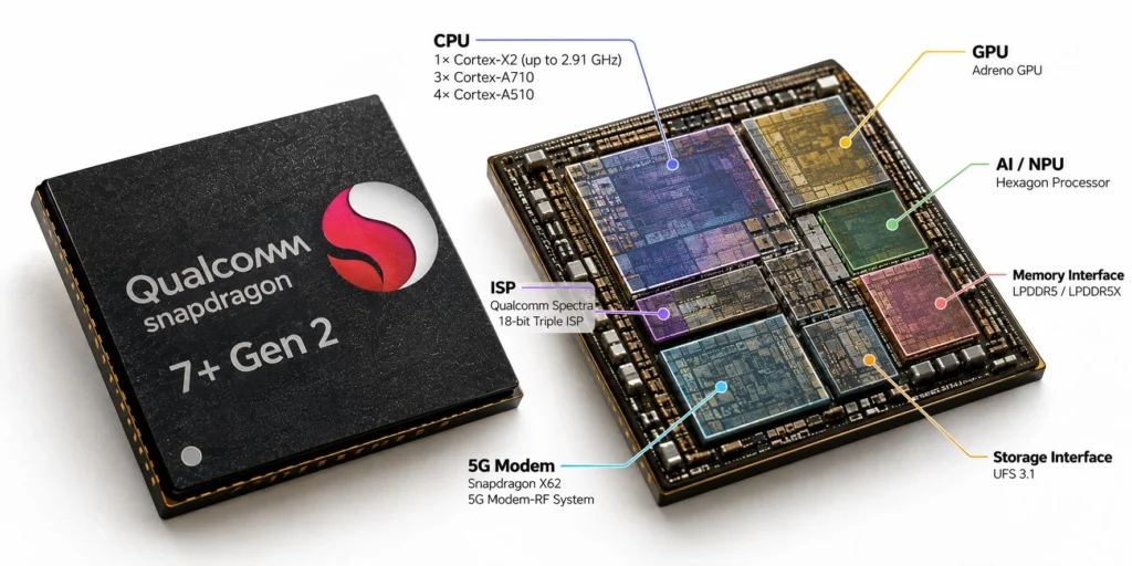
इसी वजह से इसकी anatomy को समझने का सही तरीका specification sheet को ऊपर से नीचे पढ़ना नहीं है। सवाल यह है कि जब कोई game चलता है, camera photo लेता है, AI workload process होता है या phone 5G से जुड़ता है, तब इस chip के कौन-कौन से हिस्से एक-दूसरे के साथ काम करते हैं?
सबसे पहले CPU: 1+3+4 configuration क्यों मायने रखता है?
Snapdragon 7+ Gen 2 का CPU 64-bit Qualcomm Kryo CPU है। इसमें एक prime core, तीन performance cores और चार efficiency cores हैं।
| CPU Block | Configuration |
|---|---|
| Prime core | 1 × up to 2.91GHz |
| Performance cores | 3 × up to 2.49GHz |
| Efficiency cores | 4 × up to 1.8GHz |
| Total | 8 cores |
| Architecture | 64-bit |
| Process | 4nm |
Qualcomm ने previous Snapdragon 7-series generation की तुलना में up to 50% higher CPU performance का दावा किया था। ये Qualcomm का generational comparison है; इसे हर smartphone या हर benchmark में मिलने वाला fixed result नहीं समझना चाहिए।
CPU का काम केवल app खोलना नहीं है। Android के system tasks, app logic, game physics, background processes और बहुत से general-purpose calculations इसी तरह के CPU cores पर चलते हैं।
Prime core ज्यादा demanding bursts के लिए useful हो सकता है, performance cores sustained heavier workloads संभाल सकते हैं और efficiency cores relatively lighter workloads को कम power में process करने में मदद करते हैं।
लेकिन operating system का scheduler workload और thermal/power conditions देखकर cores का इस्तेमाल करता है। इसलिए यह कहना सही नहीं होगा कि “heavy काम हमेशा prime core पर और light काम हमेशा efficiency core पर चलता है।”
GPU में 2× jump का मतलब सिर्फ ज्यादा FPS नहीं है
Snapdragon 7+ Gen 2 में Qualcomm का Adreno GPU है। Qualcomm ने previous 7-series generation की तुलना में up to 2× GPU performance का दावा किया था। साथ ही company ने gaming में select Snapdragon Elite Gaming features भी शामिल किए।
इनमें Auto Variable Rate Shading (VRS) खास है। Game में screen के हर हिस्से को समान rendering detail की जरूरत नहीं होती। VRS की मदद से important areas को higher shading rate पर और कम important areas को lower rate पर render किया जा सकता है। इससे GPU workload और power consumption को balance करने में मदद मिलती है।
Platform में Physically Based Rendering, Volumetric Rendering और Adreno Frame Motion Engine जैसी gaming capabilities भी दी गई थीं। Qualcomm ने HDR gaming और Vulkan 1.1 support भी list किया है।
GPU का role इसलिए सिर्फ “graphics बनाना” नहीं है। CPU game logic और data preparation संभाल सकता है, memory assets उपलब्ध कराती है और GPU उन्हें frames में बदलता है। Display subsystem आखिर में उन frames को screen तक पहुँचाता है।
Memory subsystem: CPU और GPU को data कौन देता है?
Snapdragon 7+ Gen 2 LPDDR5 memory up to 3200MHz support करता है और memory capacity up to 16GB तक listed है। Storage side पर UFS 3.1 support दिया गया है।
RAM में currently active applications और processing data रहता है। UFS storage में apps, photos, videos और बाकी permanent data रखा जाता है।
जब कोई game launch होती है, storage से जरूरी files memory में आती हैं। CPU game logic process करता है और GPU को rendering के लिए data मिलता है। AI workload में model data भी memory subsystem के जरिए accelerator तक पहुँचता है।
Snapdragon 7+ Gen 2 की anatomy में memory controller और memory interface कोई secondary detail नहीं हैं; वे compute blocks और बाकी system के बीच data movement का हिस्सा हैं।
AI Engine में आखिर क्या है?
Snapdragon 7+ Gen 2 का AI architecture केवल एक simple “NPU” block नहीं है।
Qualcomm के official brief में Hexagon Processor के साथ Hexagon Scalar Accelerator, Hexagon Tensor Accelerator, Hexagon Vector eXtensions (HVX), Fused AI Accelerator architecture, और INT8, INT16 व FP16 precision support listed हैं। इसके साथ Qualcomm Sensing Hub भी platform का हिस्सा है।
Qualcomm ने previous generation की तुलना में up to 2× AI performance और up to 40% better performance per watt का claim किया था।
उदाहरण के लिए image processing में AI-based face detection, autofocus या auto-exposure जैसे काम हो सकते हैं। Sensing Hub low-power sensor और contextual workloads के लिए useful है, जहाँ हर छोटी activity के लिए main CPU/GPU को fully active करना जरूरी नहीं होता।
इससे AI block का role केवल future generative AI तक सीमित नहीं रहता। Smartphone में AI पहले से camera, voice, sensors और system intelligence के कई हिस्सों में इस्तेमाल हो रहा था।
Sensing Hub को अलग से समझना जरूरी है
Chip anatomy में Sensing Hub को सिर्फ AI Engine के नीचे एक छोटा नाम लिखकर छोड़ना ठीक नहीं होगा।
इसका उद्देश्य low-power context processing में मदद करना है। ऐसे workloads में sensors, audio और दूसरे contextual signals से information आ सकती है। इस तरह का architecture battery बचाने में useful हो सकता है क्योंकि हर छोटी sensor-related calculation के लिए high-performance CPU या GPU को जगाना जरूरी नहीं पड़ता।
Snapdragon 7+ Gen 2 में AI का एक हिस्सा high-performance compute के लिए है और दूसरा हिस्सा low-power always-aware type workloads के लिए काम कर सकता है। Qualcomm के official brief में Sensing Hub को AI architecture के साथ separately list किया गया है।
Camera anatomy में सबसे बड़ा हिस्सा: 18-bit Spectra ISP
Snapdragon 7+ Gen 2 में Qualcomm Spectra Triple 18-bit ISP है।
Qualcomm ने इसे 7-Series में पहली 18-bit ISP implementation के रूप में highlight किया था और company के अनुसार यह 14-bit ISP की तुलना में 4,000× से ज्यादा camera data capture कर सकता है।
यह number सुनकर एक बात साफ रखनी चाहिए: इसका मतलब photo quality 4,000× बेहतर होना नहीं है। 18-bit processing का मतलब है कि ISP ज्यादा image information और dynamic range data को process कर सकता है। Final photo फिर भी sensor, lens, exposure, HDR algorithms और phone manufacturer’s computational photography पर depend करती है।
| Camera capability | Support |
|---|---|
| ISP | Triple 18-bit Spectra ISP |
| Computer vision ISP | Up to 3.0 Gigapixels/sec |
| Maximum photo capture | Up to 200MP |
| Triple camera | Up to 32MP + 32MP + 32MP @ 30FPS with ZSL |
| Dual camera | Up to 64MP + 36MP @ 30FPS with ZSL |
| Single camera | Up to 108MP @ 30FPS with ZSL |
| HDR | Multi-frame / staggered HDR support |
| Video | 4K HDR @ 60FPS |
| Slow motion | 1080p @ 240FPS |
ये chipset-level capabilities हैं; actual smartphone में manufacturer इनमें से सिर्फ कुछ capabilities implement कर सकता है।
Mega Low Light: ISP और AI की partnership
Low-light photography में Snapdragon 7+ Gen 2 का Mega Low Light feature खास था।
Qualcomm के अनुसार system 30 images तक की information combine करके brighter और clearer final image बनाने की कोशिश करता है।
यहाँ camera sensor अकेला काम नहीं कर रहा। Sensor frames capture करता है, ISP image data process करता है और computational photography algorithms अलग-अलग frames की useful information को combine करते हैं।
इसीलिए low-light result को केवल megapixel count से judge करना गलत है — Sensor + ISP + AI/software processing + lens + exposure control मिलकर final image बनाते हैं।
Video pipeline भी अलग hardware मांगती है
Snapdragon 7+ Gen 2 में 4K HDR video capture up to 60FPS support है। Qualcomm के brief में HDR10+, HDR10, HLG और Dolby Vision video formats listed हैं। 10-bit HEIF/HEIC photo और HEVC video capture support भी दिया गया है।
Playback side पर hardware-accelerated H.265 और VP9 decoding तथा HDR10+, HDR10, HLG और Dolby Vision playback support दिया गया है।
यह media hardware CPU को हर frame का पूरा decode/encode workload अकेले करने से बचाता है। Gaming में GPU important है, लेकिन video playback और recording में dedicated media blocks और ISP ज्यादा relevant हो जाते हैं।
Display subsystem को भूलना भी सही नहीं होगा
Snapdragon 7+ Gen 2 on-device display पर 4K @ 60Hz और QHD+ @ 120Hz तक support करता है।
External display support भी 4K @ 60Hz तक है। Qualcomm ने 10-bit color depth, Rec. 2020 और HDR10/HDR10+ support भी list किया है।
इसका मतलब यह नहीं कि हर Snapdragon 7+ Gen 2 phone में QHD+ 120Hz panel होगा। Manufacturer अपनी device cost, battery और display design के हिसाब से अलग panel लगा सकता है, लेकिन SoC level पर इतना headroom मौजूद था।
5G modem: X62 सिर्फ internet speed का नाम नहीं है
Snapdragon 7+ Gen 2 में Snapdragon X62 5G Modem-RF System है।
Official specification के अनुसार peak download speed up to 4.4Gbps है। यह 5G mmWave और sub-6GHz दोनों को support करता है, साथ ही SA और NSA modes भी।
Modem side पर mmWave 4 carriers के साथ 2×2 MIMO, Sub-6GHz पर 4×4 MIMO, Dynamic Spectrum Sharing, 5G PowerSave 2.0, Smart Transmit 2.0, Wideband Envelope Tracking, AI-Enhanced Signal Boost, Global 5G Multi-SIM और 5G/4G Dual-SIM Dual Active जैसी capabilities दी गई थीं।
इसलिए modem को केवल “4.4Gbps वाला block” समझना गलत होगा। यह radio conditions, bands, antennas, power और network connection के बीच लगातार काम करने वाला पूरा subsystem है।
Wi-Fi और Bluetooth के लिए FastConnect 6900
Cellular modem के अलावा Snapdragon 7+ Gen 2 में Qualcomm FastConnect 6900 system है।
यह Wi-Fi 6E support करता है और Qualcomm के अनुसार peak Wi-Fi speed 3.6Gbps तक है। 2.4GHz, 5GHz और 6GHz bands तथा 20/40/80/160MHz channel bandwidths supported हैं।
Bluetooth side पर Bluetooth 5.3 और Snapdragon Sound-related capabilities दी गई हैं, जिसमें aptX Voice, aptX Lossless, aptX Adaptive और LE Audio support शामिल है।
इससे पता चलता है कि SoC platform में connectivity केवल cellular modem तक सीमित नहीं है।
Location system भी इसी anatomy का हिस्सा है
Snapdragon 7+ Gen 2 में GPS, GLONASS, BeiDou, Galileo, QZSS और NavIC capability listed है।
इसके अलावा dual-frequency GNSS (L1/L5) और sensor-assisted positioning भी support करता है। Qualcomm ने urban pedestrian navigation और lane-level vehicle navigation जैसे use cases भी document किए हैं।
Navigation में सिर्फ satellite signal नहीं होता। Phone के sensors और positioning algorithms भी location को ज्यादा useful बनाने में योगदान देते हैं।
Security layer: chip की invisible लेकिन जरूरी anatomy
Snapdragon 7+ Gen 2 में security के लिए कई layers हैं — Platform Security Foundations, Trusted Execution Environment and Services, Trust Management Engine, Qualcomm Wireless Edge Services, Qualcomm Type-1 Hypervisor और Premium security features। Official brief में ये components अलग security layer के रूप में listed हैं।
इसका मतलब smartphone security केवल fingerprint sensor नहीं है। Secure execution, trusted software environment, key management और isolated system resources जैसे mechanisms chip/platform level पर महत्वपूर्ण होते हैं।
Snapdragon 7+ Gen 2 compatible devices में Qualcomm 3D Sonic और 3D Sonic Max fingerprint sensor technologies का support भी listed है।
USB, Audio, Charging — छोटे पर जरूरी blocks
Qualcomm के product brief में USB 3.1 और USB Type-C support listed है। इस तरह के I/O interfaces SoC को external peripherals और device-level data paths के साथ communicate करने देते हैं।
Audio side पर Qualcomm Aqstic audio codec और Aqstic smart speaker amplifier support है, साथ ही Snapdragon Sound technology के साथ aptX Voice, aptX Lossless, aptX Adaptive और LE Audio capabilities भी listed हैं।
Charging के लिए Snapdragon 7+ Gen 2 Quick Charge 5 Technology support करता है। लेकिन fast charging को केवल SoC feature मानना सही नहीं होगा — actual charging behavior में charger, charging IC/PMIC, battery, thermal sensors और phone manufacturer’s implementation भी शामिल होते हैं।
इसी तरह SoC की power efficiency का असर पूरे phone पर पड़ता है, लेकिन final battery life केवल processor तय नहीं करता। Screen, modem usage, camera, gaming, background apps, battery capacity और thermal design भी equally important हैं।
Physical anatomy: package के अंदर वास्तव में क्या पता है?
यहाँ Chip Anatomy में सबसे ज्यादा सावधानी जरूरी है।
Snapdragon 7+ Gen 2 एक semiconductor package के रूप में phone motherboard पर लगाया जाता है। उसके अंदर silicon die पर CPU, GPU, AI, ISP, connectivity और दूसरे functional blocks मौजूद होते हैं।
लेकिन Qualcomm ने public documentation में इसका complete transistor-level floorplan, exact die area या हर block की exact physical position disclose नहीं की है। इसलिए visual में exact silicon placement invent करना सही नहीं होगा।
| Physical / Functional Layer | Role |
|---|---|
| Package | SoC को motherboard से electrically connect करना |
| Silicon die | Main semiconductor logic |
| Kryo CPU cluster | General-purpose computing |
| Adreno GPU | Graphics और parallel workloads |
| Hexagon AI subsystem | AI/ML processing |
| Sensing Hub | Low-power contextual processing |
| Spectra ISP | Camera/image processing |
| Video/media hardware | Encode/decode और media processing |
| Display subsystem | Display output processing |
| Memory controller | LPDDR5 communication |
| Storage interface | UFS 3.1 communication |
| X62 Modem-RF | Cellular communication |
| FastConnect 6900 | Wi-Fi/Bluetooth |
| GNSS subsystem | Positioning |
| Security subsystem | Trusted execution/security |
| I/O | USB और external data connections |
| Power-related interfaces | Power/performance management ecosystem |
यह table functional anatomy है, exact silicon floorplan नहीं।
एक game चलाते समय कौन-कौन से blocks काम करते हैं?
मान लीजिए कोई demanding 3D game चल रही है।
CPU game logic, physics और system-level tasks संभालता है। Memory game assets और active data रखती है। GPU frames render करता है। VRS जैसे features GPU workload को optimize कर सकते हैं। Display subsystem final frames screen तक पहुँचाता है।
अगर game में network multiplayer है, तो Wi-Fi या 5G subsystem भी लगातार active रहेगा। अगर AI-based feature इस्तेमाल हो रहा है, तो Hexagon AI architecture workload के relevant हिस्से को accelerate कर सकता है। और इन सबके बीच power और thermal management यह तय करने में मदद करते हैं कि device कितनी देर तक उस performance level को sustain कर पाएगा।
Camera app खोलने पर कहानी अलग हो जाती है। Sensor image data capture करता है, Spectra ISP उसे process करता है, AI-based face detection, autofocus और auto-exposure जैसे functions AI processing से जुड़े हो सकते हैं, multi-frame noise reduction और HDR जैसे operations कई frames की information को combine कर सकते हैं। फिर processed image display पर दिखाई जा सकती है या UFS storage में save हो सकती है।
Snapdragon 7+ Gen 2 की सबसे बड़ी limitation क्या थी?
Snapdragon 7+ Gen 2 को उस समय 7-Series का high-end platform माना गया था, लेकिन इसे Snapdragon 8-series flagship SoC का direct equivalent कहना सही नहीं होगा।
इसकी positioning ही यह बताती है कि Qualcomm 7-Series में flagship-style performance और features के कुछ हिस्से नीचे ला रहा था। लेकिन architecture, platform features और overall positioning में यह 8-Series का replacement नहीं था।
एक manufacturer बेहतर cooling लगा सकता है। दूसरा अधिक aggressive power limits रख सकता है। किसी phone में बड़ा camera sensor होगा, किसी में छोटा। RAM, storage, display और software optimization भी अलग होंगे। इसलिए Snapdragon 7+ Gen 2 वाला हर smartphone बिल्कुल एक जैसा perform करेगा, यह मानना सही नहीं है।
7+ Gen 2 के बाद दिशा कहाँ बदली?
इस chip की anatomy को समझने का एक अच्छा तरीका इसकी अगली generation देखना है।
2024 में Qualcomm ने Snapdragon 7+ Gen 3 पेश किया। उसमें company ने on-device generative AI को 7-Series में आगे बढ़ाया, Wi-Fi 7 जोड़ा और Snapdragon 7+ Gen 2 की तुलना में 15% CPU और 45% GPU performance improvement का claim किया। 7+ Gen 3 में Snapdragon X63 modem, Wi-Fi 7 और ज्यादा advanced AI architecture के साथ Micro Tile Inferencing और Hexagon Direct Link जैसी capabilities भी आईं।
7+ Gen 2 में Qualcomm ने CPU/GPU performance के साथ AI, camera और connectivity को काफी ऊपर push किया था। अगली generation में AI को और central role मिला — यह future prediction नहीं है, 7+ Gen 3 के actual architecture में यह direction दिखाई देती है।
तो Snapdragon 7+ Gen 2 की असली anatomy क्या बताती है?
Snapdragon 7+ Gen 2 को केवल इन numbers से याद करना आसान है: 2.91GHz CPU, 2× GPU performance, 18-bit ISP और 4.4Gbps 5G।
इसके अंदर 1+3+4 Kryo CPU, Adreno GPU, Hexagon AI architecture, Sensing Hub, 18-bit Spectra Triple ISP, video/media processing, LPDDR5 memory controller, UFS 3.1 interface, X62 5G Modem-RF, FastConnect 6900, GNSS, security subsystem, USB/I/O, audio subsystem, display pipeline और Quick Charge 5 support — ये सब मिलकर एक integrated mobile platform बनाते हैं।
इन blocks की सबसे महत्वपूर्ण बात उनकी individual specification नहीं, बल्कि उनका आपसी connection है। Gaming में CPU, memory, GPU और display साथ आते हैं। Camera में sensor, ISP, AI और memory जुड़ते हैं। AI workloads में Hexagon, memory और software एक साथ काम करते हैं। 5G use में modem, RF, antennas, power management और network stack एक system बनाते हैं।
यह वह generation थी जहाँ Qualcomm ने premium smartphone experience को केवल CPU/GPU performance से आगे ले जाकर AI, computational photography, gaming, connectivity और power efficiency के एक साथ काम करने वाले platform के रूप में push किया। और 7+ Gen 3 में वही direction आगे बढ़कर on-device generative AI और Wi-Fi 7 तक पहुँची।
Source: Qualcomm Snapdragon 7+ Gen 2 Official Product Page & Mobile Platform Product Brief, Snapdragon 7+ Gen 3 Official Product Information (for generational context).
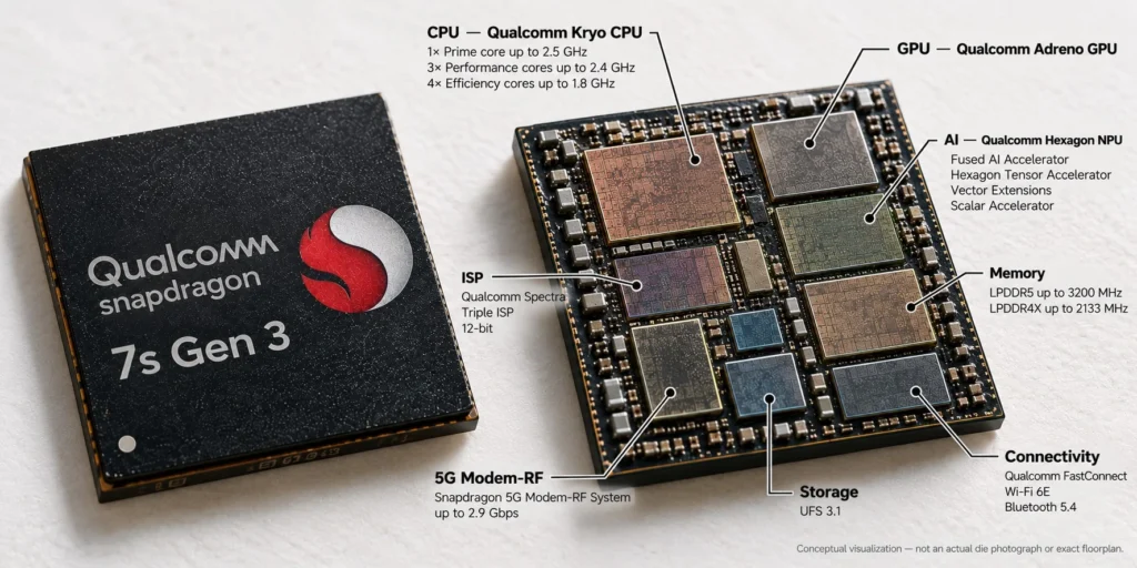
Qualcomm ने Snapdragon 7s Gen 3 को 7-Series के उस “s” segment में रखा है, जहाँ कंपनी कुछ चुनिंदा high-end technologies को ज्यादा affordable smartphones तक लाने की कोशिश करती है। इसी वजह से इसका focus सिर्फ raw CPU speed पर नहीं है।
इस chip में CPU, GPU और AI engine तीनों को साथ लेकर चलने की कोशिश दिखाई देती है। Qualcomm के अनुसार Snapdragon 7s Gen 3 में predecessor के मुकाबले CPU performance करीब 20%, GPU performance up to 40% और AI performance 30% से ज्यादा बढ़ी, जबकि overall power consumption में 12% तक सुधार बताया गया है। ये numbers अपने आप में कहानी पूरी नहीं बताते; असली बात यह है कि ये बदलाव chip के अलग-अलग हिस्सों के बीच कैसे बंटे हैं।
सबसे पहले CPU को देखें
Snapdragon 7s Gen 3 का CPU Qualcomm की 64-bit Kryo CPU architecture पर आधारित है। इसमें तीन अलग-अलग तरह के core groups हैं:
| CPU Cluster | Core Count | Maximum Clock |
|---|---|---|
| Prime | 1 | Up to 2.5 GHz |
| Performance | 3 | Up to 2.4 GHz |
| Efficiency | 4 | Up to 1.8 GHz |
इसका मतलब configuration 1 + 3 + 4 है। कुल आठ CPU cores हैं। Qualcomm ने इस platform को 4nm process technology पर बनाया है।
यहाँ एक छोटी लेकिन जरूरी बात है। Qualcomm की public specifications इन cores को Prime, Performance और Efficiency groups के रूप में बताती हैं, लेकिन इनके exact underlying CPU core designs को इस brief में अलग से identify नहीं किया गया है। इसलिए केवल अनुमान के आधार पर किसी specific Cortex core का नाम जोड़ना सही नहीं होगा।
CPU का काम सिर्फ benchmark score बढ़ाना नहीं है। फोन में कोई app खोलना, background में कई apps रखना, browser में tabs चलाना, photo processing के दौरान system tasks संभालना या game के दौरान अलग-अलग background processes चलाना — इन सबमें CPU लगातार काम करता है।
Prime core का ज्यादा clock speed वाला हिस्सा short, demanding workloads में मदद करता है। Performance cores sustained या parallel workloads संभालते हैं, जबकि efficiency cores comparatively हल्के कामों को कम power में चलाने के लिए होते हैं। यही 1+3+4 arrangement Snapdragon 7s Gen 3 की power strategy का पहला हिस्सा है।
GPU सिर्फ gaming के लिए नहीं है
CPU के साथ दूसरा बड़ा block है Qualcomm Adreno GPU। Qualcomm के मुताबिक Snapdragon 7s Gen 3 में पिछले generation की तुलना में GPU performance up to 40% तक बढ़ी है। GPU OpenGL ES 3.2, OpenCL 2.0 FP और Vulkan 1.3 APIs को support करता है।
Gaming में इसका सीधा फायदा graphics rendering में मिलता है। लेकिन modern smartphone में GPU का इस्तेमाल सिर्फ game frames बनाने तक सीमित नहीं है।
Graphics composition, image processing के कुछ हिस्से, visual effects और display-related workloads में भी GPU की भूमिका हो सकती है। Snapdragon 7s Gen 3 का visual subsystem HDR gaming और 10-bit color depth को support करता है।
Video side पर hardware-accelerated H.265 और VP9 decoding भी मौजूद है। HDR playback में HDR10, HDR10+ और HLG जैसे formats supported हैं। GPU, display और camera/video pipeline के साथ मिलकर यहाँ smartphone का पूरा visual workload संभालता है।
असली बदलाव: AI अब अलग feature नहीं रहा
Snapdragon 7s Gen 3 की सबसे दिलचस्प on-device AI है। इस platform में Qualcomm AI Engine के अंदर Hexagon processor, Hexagon Scalar Accelerator और Hexagon Vector eXtensions (HVX) जैसे blocks मौजूद हैं। Qualcomm ने AI workload के लिए Fused AI Accelerator Architecture और Hexagon Tensor Accelerator भी specify किया है। साथ ही INT4, INT8 और INT16 precision support दिया गया है।
AI processing का मतलब केवल chatbot चलाना नहीं है। Smartphone में AI पहले से camera, voice, image enhancement, object detection, noise reduction और कई background tasks में इस्तेमाल होता रहा है।
Snapdragon 7s Gen 3 में Qualcomm ने इसी direction को आगे बढ़ाया और on-device generative AI support को भी platform का हिस्सा बनाया। Qualcomm के अनुसार AI performance previous generation की तुलना में 30% से ज्यादा बेहतर हुई है।
On-device processing का फायदा यह है कि हर AI task के लिए cloud server पर data भेजना जरूरी नहीं पड़ता। जिस workload को phone locally संभाल सकता है, उसे वहीं process किया जा सकता है। इससे response time, connectivity dependency और कुछ use cases में privacy के लिहाज से भी फायदा हो सकता है।
लेकिन इसका मतलब यह नहीं है कि Snapdragon 7s Gen 3 हर बड़े generative-AI model को बिना किसी limitation के phone पर चला देगा। Actual capability model के size, quantization, RAM, software optimization और OEM implementation पर निर्भर करेगी।
AI engine अकेला काम नहीं करता
मान लीजिए camera में कोई object detect करना है। Image sensor data पहले ISP pipeline में आता है। वहाँ image processing होती है। फिर machine-learning based processing किसी stage पर AI acceleration का इस्तेमाल कर सकती है। इसके बाद CPU/GPU और बाकी system blocks result को application तक पहुंचाने में भूमिका निभाते हैं।
Snapdragon 7s Gen 3 में Qualcomm Sensing Hub भी मौजूद है। Qualcomm इसके साथ sensor और audio workloads के लिए dedicated low-power AI processing capabilities बताता है।
इसका practical मतलब यह है कि हर छोटी sensing या always-on task के लिए बड़े CPU cores को लगातार जगाने की जरूरत नहीं होनी चाहिए। यही वह जगह है जहाँ performance और battery efficiency का balance दिखाई देता है।
Camera में AI और ISP का connection
Snapdragon 7s Gen 3 में Qualcomm Spectra ISP दिया गया है, जिसमें triple 12-bit ISPs हैं। Platform single camera में up to 200MP photo capture support करता है। इसके अलावा 4K HDR video capture और 1080p पर 120fps slow-motion capture भी supported है।
लेकिन 200MP support को देखकर यह मान लेना कि हर phone इसी quality की 200MP photos बनाएगा, सही नहीं होगा। Camera result सिर्फ ISP पर निर्भर नहीं करता। Sensor quality, lens, memory bandwidth, image-processing algorithms और phone manufacturer की tuning भी उतनी ही महत्वपूर्ण होती है।
Snapdragon 7s Gen 3 में AI-assisted camera features भी दिए गए हैं। Qualcomm deep-learning based face detection, facial landmark detection, autofocus और auto-exposure जैसी capabilities बताता है। Low-light photography के लिए AI De-noiser (AIDE) भी platform का हिस्सा है।
यहाँ AI कोई अलग menu feature नहीं है — वह camera pipeline के अंदर ही उपयोगी processing का हिस्सा बन जाता है।
Memory: CPU और AI के बीच का रास्ता
किसी भी modern SoC में memory subsystem को नजरअंदाज करना आसान है, जबकि high-performance workloads में इसका असर काफी बड़ा होता है।
Snapdragon 7s Gen 3 LPDDR5 memory up to 3200 MHz और LPDDR4X up to 2133 MHz को support करता है। Qualcomm maximum memory density 16GB बताता है। Storage के लिए UFS 3.1 support मौजूद है।
यहाँ CPU, GPU और AI accelerator सीधे isolated तरीके से काम नहीं करते। किसी AI workload को process करने के लिए data memory से accelerator तक पहुंचता है। Camera processing में भी image data लगातार move होता है। Gaming में textures और अन्य assets memory subsystem पर निर्भर होते हैं।
इसलिए chip की performance सिर्फ “CPU कितने GHz पर चलता है” से तय नहीं होती — memory, accelerator और processing blocks के बीच data movement भी पूरे system की responsiveness और power efficiency को प्रभावित करता है।
5G भी SoC की anatomy का हिस्सा है
Snapdragon 7s Gen 3 में Snapdragon 5G Modem-RF System integrated है। यह 5G mmWave और sub-6 GHz दोनों को support करता है और SA तथा NSA modes के साथ काम कर सकता है। Qualcomm के अनुसार peak download speed up to 2.9 Gbps है। Sub-6 GHz में 4×4 MIMO और mmWave में 2×2 MIMO support दिया गया है।
यहाँ भी सिर्फ speed number देखना पर्याप्त नहीं है। Actual network speed carrier spectrum, signal strength, device antennas और local network conditions पर निर्भर करेगी।
Power side पर Qualcomm 5G PowerSave 2.0, Smart Transmit 2.0 और Wideband Envelope Tracking जैसी technologies देता है। AI-Enhanced Signal Boost भी platform features में शामिल है — इससे modem को भी पूरे chip के power-management design का हिस्सा समझना चाहिए।
Wi-Fi और Bluetooth का अलग connectivity block
Wireless connectivity के लिए FastConnect system दिया गया है। Snapdragon 7s Gen 3 में Wi-Fi 6E support है और Qualcomm peak Wi-Fi speed up to 2.9 Gbps बताता है। 2.4GHz, 5GHz और 6GHz bands supported हैं। Bluetooth side पर Bluetooth 5.4 और LE Audio support मौजूद है।
यह हिस्सा gaming और streaming जैसे workloads में CPU/GPU जितना visible नहीं होता, लेकिन modern phone experience में इसका असर सीधा दिखाई देता है। High-speed Wi-Fi से large files, cloud data और game downloads जल्दी transfer हो सकते हैं, जबकि Bluetooth और LE Audio wireless accessories और audio devices के लिए connectivity संभालते हैं।
Display और video pipeline
Snapdragon 7s Gen 3 का on-device display support FHD+ at up to 144Hz है। External display के लिए platform up to 4K at 60Hz और 10-bit color depth के साथ HDR10/HDR10+ support करता है।
Game में GPU frames render करता है। Video playback में dedicated hardware video decoding मदद करता है। Display pipeline उस processed information को panel तक पहुंचाती है — screen पर दिखाई देने वाली final image एक single block का result नहीं होती।
Location और sensors भी इसी system का हिस्सा हैं
Navigation के लिए Snapdragon 7s Gen 3 में concurrent GPS, GLONASS, BeiDou, Galileo, QZSS और NavIC support दिया गया है। यह triple-frequency GNSS — L1/L5/L2 support करता है। Qualcomm sensor-assisted positioning और urban pedestrian तथा lane-level vehicle navigation जैसे use cases भी बताता है।
Location accuracy सिर्फ satellite signal पर निर्भर नहीं करती — sensors और positioning algorithms मिलकर movement और location estimate को refine कर सकते हैं।
Audio processing के लिए भी dedicated blocks हैं
Audio side पर Qualcomm Aqstic audio codec और Aqstic smart speaker amplifier support मौजूद है। Snapdragon 7s Gen 3 Snapdragon Sound technology suite को भी support करता है, जिसमें Qualcomm aptX Voice, aptX Lossless और aptX Adaptive जैसे audio technologies शामिल हैं।
यहाँ Sensing Hub और AI processing का connection भी बनता है। Voice-related workloads में हमेशा पूरे high-performance CPU को इस्तेमाल करना जरूरी नहीं होता — low-power sensing और audio processing blocks background interaction को ज्यादा efficiently handle कर सकते हैं।
Security layer को भूलना आसान है
SoC की anatomy सिर्फ performance blocks से पूरी नहीं होती। Snapdragon 7s Gen 3 में Trusted Execution Environment (TEE), Trust Management Engine, platform security foundations और Qualcomm Type-1 Hypervisor जैसी security technologies मौजूद हैं।
इनका काम user को सीधे दिखाई नहीं देता, लेकिन secure processing, protected environments और sensitive operations के लिए ये layers महत्वपूर्ण हैं। Modern smartphone में banking credentials, biometric information, authentication keys और private data जैसे workloads होते हैं — इसलिए security subsystem भी chip architecture का उतना ही वास्तविक हिस्सा है जितना CPU या GPU।
Charging और power management की एक जरूरी सीमा
Snapdragon 7s Gen 3 Quick Charge 4+ technology को support करता है। लेकिन यहाँ एक common confusion है। SoC में charging technology का support होने का मतलब यह नहीं है कि हर Snapdragon 7s Gen 3 phone एक ही charging speed देगा। Actual charging speed phone के PMIC, battery design, charger, thermal limits और manufacturer implementation पर निर्भर करती है।
इसी तरह Qualcomm का 12% overall power savings वाला figure platform-level comparison है; किसी specific smartphone की battery life उससे सीधे calculate नहीं की जा सकती।
Chip के अंदर physical anatomy कैसी है?
यह हिस्सा interesting है, लेकिन यहाँ speculation करना सही नहीं होगा। Snapdragon 7s Gen 3 एक 4nm mobile SoC है। इसके अंदर CPU, GPU, Hexagon AI processing, Spectra ISP, memory interfaces, connectivity, security और दूसरे system blocks silicon die पर integrated होते हैं।
लेकिन Qualcomm ने public product brief में इसका complete transistor-level floorplan या exact physical die layout publish नहीं किया है। इसलिए anatomy visual में किसी specific block की exact physical position को confirmed fact की तरह दिखाना सही नहीं होगा।
Conceptually इसे इस तरह समझ सकते हैं: Package → Silicon Die → CPU / GPU / Hexagon AI / ISP / Memory Interface / Modem & Connectivity / Security / I/O
यह functional anatomy है, exact photographic floorplan नहीं।
एक camera shot में कितने blocks साथ काम कर सकते हैं?
मान लीजिए phone से low-light photo ली गई। सबसे पहले image sensor raw data capture करता है। Data ISP तक जाता है। Spectra ISP image processing करता है। Face detection या दूसरे machine-learning based tasks के लिए AI acceleration इस्तेमाल हो सकती है। Memory subsystem बीच में data movement संभालता है। CPU overall software pipeline को coordinate करता है।
अगर photo में noise ज्यादा है तो AI-assisted denoising जैसी capability काम कर सकती है। फाइनल photograph इसलिए सिर्फ “200MP ISP” का result नहीं है — यह sensor + ISP + AI + memory + CPU + software tuning का combined output है।
Gaming में picture थोड़ी अलग है
Game शुरू करने पर CPU game logic, operating-system tasks और कई background operations संभालता है। GPU rendered frames तैयार करता है। Memory subsystem textures और game data को feed करता है। Display pipeline final frames को screen तक पहुंचाती है।
इस पूरी process में AI हर frame को generate नहीं कर रहा होता। लेकिन modern games और smartphone features में AI-assisted functions अलग-अलग जगह इस्तेमाल हो सकते हैं। इसलिए Snapdragon 7s Gen 3 का AI engine gaming performance का replacement नहीं है — उसका काम अलग है। Qualcomm का reported up to 40% GPU performance improvement इसी वजह से AI performance से अलग देखना चाहिए।
“s” नाम का मतलब समझना भी जरूरी है
Snapdragon 7s Gen 3 को देखकर इसे Snapdragon 7+ Gen 3 के साथ सीधे बराबर रखना सही नहीं होगा। Qualcomm खुद “s” segment को 7-Series की selected technologies को ज्यादा accessible smartphones तक लाने वाली category के रूप में describe करता है।
इसीलिए 7s Gen 3 का design एक अलग balance पर खड़ा है। इसका target यह नहीं है कि हर specification में 7+ series को पीछे छोड़ दे। इसके बजाय Qualcomm ने CPU, GPU, AI, camera, connectivity और power efficiency के बीच ऐसा package तैयार किया जिसे comparatively affordable devices में इस्तेमाल किया जा सके।
7s Gen 3 में असली बदलाव कहाँ दिखता है?
अगर पूरी chip को एक साथ देखें तो कहानी सिर्फ 2.5GHz CPU की नहीं है। एक तरफ CPU में करीब 20% performance improvement का दावा है। दूसरी तरफ GPU में up to 40% improvement और AI में 30% से ज्यादा improvement बताया गया है। साथ में Qualcomm 12% overall power savings का भी दावा करता है।
Qualcomm ने इसलिए सिर्फ CPU को तेज करने की कोशिश नहीं की। AI को camera और on-device workloads में ज्यादा practical बनाया गया। Sensing Hub जैसे low-power components ने background tasks के लिए अलग रास्ता दिया। ISP ने high-resolution camera और AI-assisted processing को support किया। GPU ने graphics workload संभाला और connectivity blocks ने 5G/Wi-Fi को उसी overall power envelope में चलाने की कोशिश की।
यह पूरा balance ही Snapdragon 7s Gen 3 की असली पहचान है।
आगे चलकर mobile SoCs में यह approach और ज्यादा relevant होती जा रही है। Generative AI, local image editing, voice processing और contextual features बढ़ रहे हैं, लेकिन हर workload के लिए बड़े CPU cores चलाना battery के लिए अच्छा रास्ता नहीं है।
इसलिए आने वाले chips में सवाल सिर्फ यह नहीं रहेगा कि CPU कितना तेज है। सवाल यह भी होगा कि सही काम के लिए chip के अंदर कौन-सा accelerator इस्तेमाल हो रहा है, data कहाँ जा रहा है और वह काम कितनी power में पूरा हो रहा है। Snapdragon 7s Gen 3 इसी बदलाव का एक practical example है।
Source: Qualcomm Snapdragon 7s Gen 3 Mobile Platform Product Brief & Official Product Information.
Snapdragon 8 Gen 2 को देखकर सबसे पहले एक चीज ध्यान खींचती है: इसका CPU 1+4+3 configuration में था। एक Prime core, चार Performance cores और तीन Efficiency cores।
पिछली पीढ़ी के Snapdragon 8 Gen 1 में 1+3+4 arrangement था। यानी Qualcomm ने एक efficiency core हटाकर एक अतिरिक्त performance core लगाया। यही छोटा-सा बदलाव 8 Gen 2 के पूरे CPU design की दिशा बताता है। Qualcomm ने इसी नए arrangement को अपनी नई Kryo CPU architecture का हिस्सा बताया था। लेकिन 8 Gen 2 की कहानी सिर्फ CPU में नहीं है।
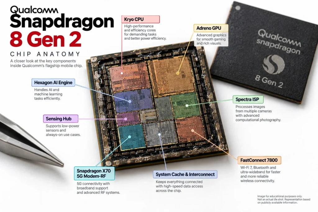
इसके अंदर GPU का design बदला, AI को chip के कई हिस्सों में फैलाया गया, camera processing को ज्यादा intelligent बनाया गया और 5G modem तक में AI processing जोड़ी गई। और जब इस chip की physical floorplan को देखा जाता है, तब इसकी anatomy और भी दिलचस्प हो जाती है।
पहले CPU को देख लेते हैं
Snapdragon 8 Gen 2 का CPU Qualcomm Kryo नाम से आया था।
इसके अंदर:
| हिस्सा | संख्या | अधिकतम frequency |
|---|---|---|
| Prime core | 1 | 3.2 GHz |
| Performance cores | 4 | 2.8 GHz |
| Efficiency cores | 3 | 2.0 GHz |
Prime core Arm Cortex-X3 technology पर आधारित था। Qualcomm के product brief में यही मूल SM8550-AB configuration दी गई है; अलग platform versions में maximum frequency अलग हो सकती है।
इस arrangement का मतलब सीधा है। अगर फोन को किसी बहुत भारी single-threaded काम में तेजी चाहिए, तो सबसे तेज Prime core सामने आता है।
अगर कई काम एक साथ चल रहे हैं, तो चार performance cores ज्यादा काम संभाल सकते हैं। और जब काम हल्का हो, तो तीन efficiency cores कम power में उसे चला सकते हैं। यानी Qualcomm ने केवल cores की संख्या नहीं बदली थी। उसने यह बदला कि chip अपना available CPU power किस तरह बांटे।
1+4+3 क्यों दिलचस्प था
मान लो फोन में कोई बड़ा app खुल रहा है। उसके साथ background में notifications, network activity और दूसरे छोटे tasks भी चल रहे हैं।
ऐसे में हर काम को सबसे तेज core पर भेजना जरूरी नहीं है। हल्का काम efficiency cores संभाल सकते हैं और ज्यादा demanding काम performance cluster में जा सकता है।
Qualcomm ने 8 Gen 2 के लिए पिछली पीढ़ी की तुलना में CPU performance में सुधार और 40% तक बेहतर power efficiency का दावा किया था। ये Qualcomm के अपने comparison numbers हैं, इसलिए इन्हें universal real-world result नहीं समझना चाहिए।
फिर GPU की बारी आती है
इस पीढ़ी में graphics performance के साथ एक ऐसी चीज आई जो उस समय Android smartphone chips में खास महत्व रखती थी: hardware-accelerated real-time ray tracing।
Ray tracing का काम केवल frame को तेज बनाना नहीं है। इसका इस्तेमाल light, reflection और shadow जैसी चीजों को ज्यादा realistic तरीके से calculate करने में होता है।
Qualcomm ने 8 Gen 2 के Adreno GPU के लिए पिछली पीढ़ी की तुलना में 25% तक faster graphics rendering और 45% बेहतर power efficiency का दावा किया था।
TechInsights की floorplan analysis के अनुसार 8 Gen 2 में पिछली पीढ़ी की तुलना में बड़ा GPU area और कुछ नए logic blocks दिखाई देते हैं। TechInsights ने यह भी अनुमान लगाया कि thermal limits को संभालने के लिए GPU clock को कम रखा गया हो सकता है। यह हिस्सा Qualcomm का official specification नहीं, बल्कि TechInsights की independent analysis है।
यही फर्क है official specification और chip analysis के बीच — एक बताता है कि manufacturer क्या दावा करता है, दूसरा बताता है कि silicon को देखने पर क्या दिखाई देता है।
AI के लिए सिर्फ एक NPU नहीं था
8 Gen 2 के समय smartphone AI को केवल “NPU” कहकर समझाना ठीक नहीं होगा। Qualcomm ने अपनी AI Engine में Kryo CPU, Adreno GPU और Hexagon Processor को एक साथ इस्तेमाल किया।
Hexagon में Tensor Accelerator, Vector Extensions, Scalar Accelerator और Micro Tile Inferencing जैसी technologies थीं। Qualcomm ने इस generation में INT4 support भी जोड़ा था।
Micro Tile Inferencing का उद्देश्य neural-network processing में data को छोटे हिस्सों में संभालना था, जिससे memory traffic और computation को ज्यादा efficiently manage किया जा सके।
Qualcomm ने कुछ AI workloads में पिछली पीढ़ी की तुलना में 4.35 गुना तक AI performance improvement का दावा किया था। यह संख्या specific workloads और MobileBERT जैसे test conditions से जुड़ी थी, इसलिए इसे हर तरह के AI काम की 4.35x speed समझना सही नहीं होगा।
AI camera तक पहुंच गया था
8 Gen 2 में Qualcomm Spectra ISP था, लेकिन camera processing को केवल traditional ISP काम की तरह नहीं रखा गया। यहां Cognitive ISP आया। इसका एक महत्वपूर्ण काम real-time semantic segmentation था। साधारण भाषा में कहें तो camera frame में अलग-अलग चीजों को पहचानकर उनके हिसाब से processing की जा सकती थी।
आसमान, चेहरा, बाल, कपड़े और background जैसी चीजों को एक ही तरीके से process करने के बजाय system scene के अलग हिस्सों के लिए अलग processing कर सकता था।
Qualcomm ने 18-bit triple Cognitive ISPs और 3.2 gigapixels per second processing capability के साथ 200MP तक single capture support बताया था। इसका मतलब यह नहीं कि हर Snapdragon 8 Gen 2 फोन का camera 200MP पर समान quality देगा — sensor, lens, OEM tuning और software processing भी final photograph में बड़ा फर्क डालते हैं।
Sensing Hub चुपचाप अपना काम करता था
अगर सिर्फ कोई sensor event देखना है, आवाज सुननी है या low-power background sensing करनी है, तो पूरी chip को high-performance state में रखने का कोई फायदा नहीं।
इसी काम के लिए Qualcomm ने Sensing Hub में dual AI processors दिए। यह audio और sensors जैसे low-power workloads संभाल सकता था और Always-Sensing Camera जैसी functionality के साथ भी काम करता था। यह हिस्सा शायद gaming benchmark में नजर नहीं आता, लेकिन battery life के लिए ऐसे low-power blocks महत्वपूर्ण होते हैं।
5G modem भी इसी कहानी का हिस्सा था
Snapdragon 8 Gen 2 के साथ Snapdragon X70 5G Modem-RF System दिया गया था। यह केवल network connection देने वाला block नहीं था। Qualcomm ने X70 में 5G AI Processor और AI-enhanced signal processing जैसी technologies शामिल की थीं।
Qualcomm के अनुसार platform की peak download speed 10 Gbps तक और upload speed 3.5 Gbps तक थी। लेकिन वास्तविक speed हमेशा इतनी नहीं होगी — network, carrier, spectrum, signal strength और device implementation पर actual result निर्भर करता है।
इसके साथ FastConnect 7800 connectivity system था, जिसमें Wi-Fi 7 और High Band Simultaneous Multi-Link जैसी capabilities शामिल थीं।
Package के अंदर सिलिकॉन कैसे बंटा है
Snapdragon 8 Gen 2 को TSMC के 4nm process पर बनाया गया था। लेकिन केवल 4nm देखकर chip की physical anatomy समझना मुश्किल है।
TechInsights ने Qualcomm SM8550 Snapdragon 8 Gen 2 का digital floorplan analysis किया था। इस analysis में package और die photographs, X-ray, SEM images और die के अलग-अलग functional blocks की पहचान शामिल थी। यानी बाहर से दिखने वाली black package के अंदर एक single flat “processor” नहीं बैठा है।
वहां अलग-अलग functions के लिए silicon area बांटा गया है — CPU cluster एक जगह है, GPU का अपना बड़ा हिस्सा है, AI और दूसरे accelerators के blocks हैं, memory interfaces हैं, और बाकी connectivity तथा system functions के लिए भी circuitry मौजूद है।
Exact internal implementation का हर हिस्सा public नहीं है। Qualcomm अपने complete floorplan और हर block की detailed internal architecture प्रकाशित नहीं करता, इसलिए anatomy image में जहां public evidence उपलब्ध नहीं है, वहां exact transistor-level structure का दावा करना सही नहीं होगा।
Memory और storage को अलग समझना जरूरी है
8 Gen 2 platform LPDDR5X memory और UFS 4.0 storage को support करता था।
दोनों का काम अलग है। RAM में operating system और चल रहे applications का data रहता है। Storage में apps, photos, videos और बाकी files लंबे समय के लिए रहती हैं।
इसलिए UFS 4.0 तेज होने का मतलब यह नहीं कि फोन की RAM भी उसी चीज को करती है। CPU, GPU और AI accelerators जिस data पर काम कर रहे हैं, उसके लिए memory bandwidth महत्वपूर्ण रहती है।
8 Gen 2 में gaming सिर्फ GPU का काम नहीं था
CPU game logic और दूसरे calculations संभालता है। Memory लगातार data उपलब्ध कराती है। GPU rendering करता है। Display system तैयार frames को screen तक पहुंचाता है। और अगर game में network multiplayer है तो modem और connectivity system भी अपना हिस्सा निभाते हैं।
8 Gen 2 में hardware ray tracing और Game Post Processing Accelerator जैसे dedicated graphics features भी थे। Qualcomm के अनुसार Game Post Processing Accelerator bloom, depth of field और motion blur जैसे effects को accelerate कर सकता था।
इसलिए किसी Snapdragon chip की gaming performance को सिर्फ “GPU कितना तेज है” से समझना अधूरा है।
इस chip की असली खासियत कहां थी
Snapdragon 8 Gen 2 को खास बनाने वाली चीज कोई एक अकेला block नहीं था।
- CPU में 1+4+3 arrangement ने Qualcomm को performance और efficiency के बीच अलग balance दिया।
- Adreno GPU में ray tracing और नए graphics blocks आए।
- Hexagon और बाकी AI hardware ने AI processing को chip के कई हिस्सों तक फैलाया।
- Cognitive ISP ने camera processing को scene-aware बनाया।
- Sensing Hub ने low-power AI और sensing को अलग रास्ता दिया।
- X70 ने connectivity side पर भी AI processing जोड़ी।
इन सबको एक ही 4nm mobile platform में साथ रखना ही इसकी बड़ी architectural कहानी थी।
Snapdragon 8 Gen 2 की Anatomy एक नजर में
| हिस्सा | Snapdragon 8 Gen 2 में | मुख्य काम |
|---|---|---|
| CPU | 8 cores, 1+4+3 | General computing |
| Prime core | Cortex-X3 technology | सबसे demanding CPU tasks |
| Performance cores | 4 | भारी multi-core workloads |
| Efficiency cores | 3 | कम power वाले tasks |
| GPU | Adreno | Graphics और parallel workloads |
| Ray tracing | Hardware accelerated | Real-time lighting और reflections |
| AI | Hexagon + CPU + GPU | On-device AI processing |
| Sensing Hub | Dual AI processors | Low-power sensing और audio |
| ISP | 18-bit triple Cognitive ISP | Camera और image processing |
| Modem | Snapdragon X70 | 5G connectivity |
| Wi-Fi | FastConnect 7800 | Wi-Fi 7 और wireless connectivity |
| Memory | LPDDR5X | Working data |
| Storage | UFS 4.0 | Long-term data storage |
| Manufacturing | TSMC 4nm | Silicon fabrication |
Snapdragon 8 Gen 2 को केवल उस दौर का एक तेज Android processor कहना इसकी anatomy को छोटा कर देता है। इस chip में Qualcomm ने CPU layout से लेकर GPU, AI, camera, sensing और connectivity तक कई हिस्सों को नए तरीके से जोड़ा था।
सबसे दिलचस्प बदलाव शायद यह था कि AI को किसी एक block में बंद रखने के बजाय पूरे platform में फैलाया गया। और CPU में 1+4+3 arrangement ने यह साफ कर दिया था कि Qualcomm सिर्फ ज्यादा cores जोड़ने की कोशिश नहीं कर रहा था। वह यह तय कर रहा था कि कौन-सा काम किस तरह के core पर और कितनी power में होना चाहिए।
Source: Official Qualcomm Snapdragon 8 Gen 2 Specifications & Press Release, TechInsights SM8550 Digital Floorplan & GPU Area Analysis.
-
 Android3 weeks ago
MediaTek Dimensity 8300: मिड-रेंज से ऊपर जाने की असली कोशिश कहाँ थी?
-
 Android3 weeks ago
Dimensity 9300 की Anatomy: All Big Core डिजाइन ने स्मार्टफोन दुनिया को कैसे चौंकाया?
-
 Apple3 weeks ago
Apple M1 Chip की असली कहानी: एक चिप ने Mac को हमेशा के लिए कैसे बदल दिया?
-
 Apple3 weeks ago
Apple A17 Pro: 3nm की पहली छलांग ने iPhone की चिप में क्या बदल दिया?
-
 Android3 weeks ago
Qualcomm Snapdragon 8 Gen 2 की Anatomy: अंदर से यह चिप इतनी खास क्यों थी?
-
 Android3 weeks ago
Qualcomm Snapdragon 8 Elite: अंदर से कितनी बदली Qualcomm की सबसे ताकतवर मोबाइल चिप?
-
 Android3 weeks ago
MediaTek Dimensity 9400: एक अलग CPU strategy ने क्या बदल दिया?
-
 Android3 weeks ago
Google Tensor G4: कागज पर नहीं, असल इस्तेमाल में कैसी है ये chip?